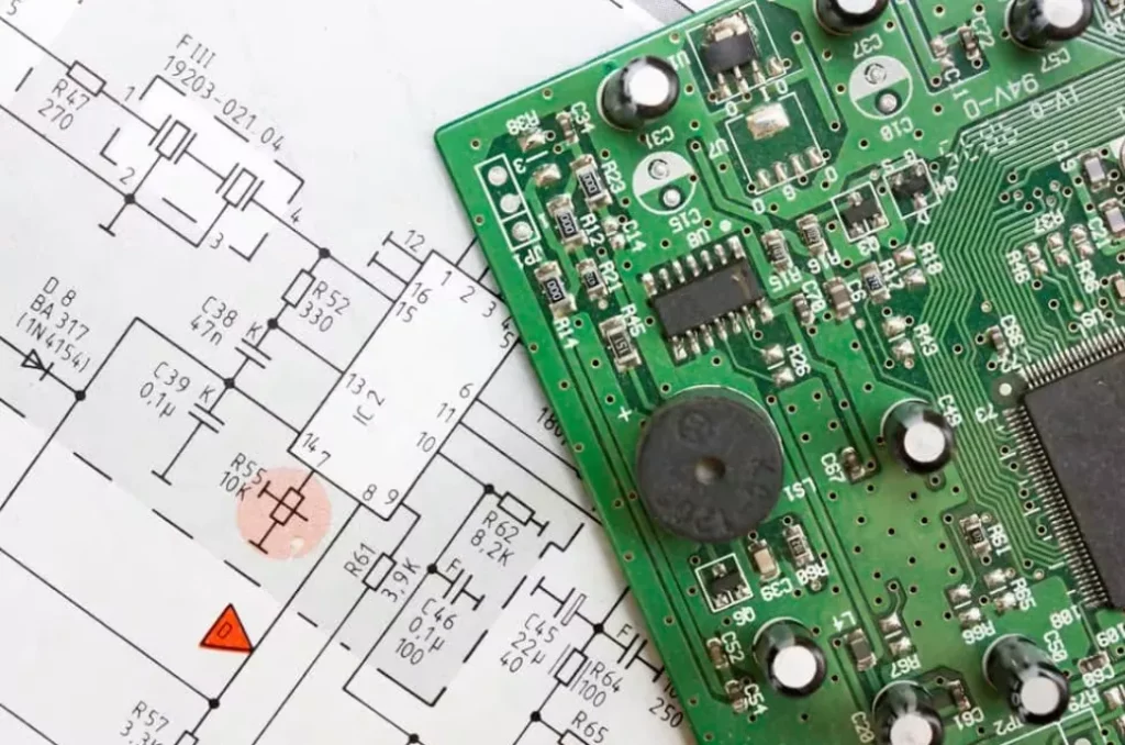
Printed circuit board (PCB) design is a complex process that integrates numerous components and layout considerations. Among the most critical aspects are the copper trace and the SOIC package. Both play a vital role in determining the performance, reliability, and manufacturability of electronic products. This article will explore how copper trace design and SOIC package selection interact within PCB manufacturing.
What Is Copper Trace in PCB?
Copper trace refers to the thin lines of copper that create the conductive pathways on a PCB. These traces connect various electronic components and allow electrical signals and power to flow throughout the board.
The width, thickness, and routing of copper traces directly affect:
• Current carrying capacity
• Signal integrity
• Heat dissipation
• EMI (Electromagnetic Interference)
• Overall PCB size and complexity
Typically, copper trace thickness is measured in ounces per square foot (oz/ft²), with common standards being 0.5 oz, 1 oz, or 2 oz copper layers. Thicker copper traces are essential for high-current or power electronics, while thinner traces are used for signal processing and compact designs.
Proper copper trace design involves careful calculation of trace width based on the expected current, using tools like PCB trace width calculators. Poorly designed traces can lead to overheating, voltage drops, or even PCB failure.
Introduction to SOIC Package
SOIC package, short for Small Outline Integrated Circuit, is a popular surface-mount package used for integrated circuits. Compared to traditional through-hole components, SOIC packages offer a much smaller footprint and lower profile, making them ideal for compact and high-density PCB layouts.
Some key characteristics of SOIC package include:
• Lead pitch typically ranging from 1.27 mm to 0.635 mm
• Easy compatibility with automated SMT assembly processes
• Reduced parasitic inductance and capacitance
• Improved high-frequency performance compared to larger packages
SOIC packages come in various pin counts, from 8 pins up to 28 or more, depending on the complexity of the integrated circuit inside.
The Interaction Between Copper Trace and SOIC Package
When designing a PCB that uses SOIC package components, copper trace layout becomes particularly important. The fine lead pitch of the SOIC package requires precise trace routing to avoid short circuits or signal integrity issues.
Key considerations include:
• Pad size and spacing must match the SOIC lead dimensions exactly to ensure reliable solder joints.
• Copper traces should be routed symmetrically to minimize skew in high-speed differential pairs.
• Trace width must be carefully calculated to handle the current without overheating, even in tight spaces.
• Via placement should avoid stress points near SOIC pads to prevent mechanical damage during thermal cycling.
The combination of fine-pitch SOIC package and proper copper trace design ensures both electrical performance and long-term reliability.
Benefits of Using Copper Trace with SOIC Package
When properly designed, the synergy between copper trace layout and SOIC package offers several benefits:
• Compact PCB footprint, allowing for smaller and lighter devices
• High signal integrity, supporting faster data transmission
• Efficient automated assembly with standard SMT equipment
• Lower manufacturing costs due to reduced board size and material usage
• Reliable thermal performance, even in densely packed circuits
Common Applications
The pairing of optimized copper trace routing with SOIC package components is widely used across various industries, such as:
• Consumer electronics (smartphones, wearables)
• Automotive electronics (control modules, sensors)
• Industrial automation (controllers, instrumentation)
• Medical devices (monitors, diagnostic equipment)
• Telecommunications (network devices, routers)
Design Challenges and Solutions
Despite the benefits, PCB designers must overcome certain challenges when working with copper trace and SOIC package configurations:
Limited Space: The tight lead pitch of SOIC requires careful trace width and spacing to avoid crosstalk and shorts.
Thermal Management: SOIC components can generate heat; adequate copper trace width and thermal vias help dissipate heat.
Manufacturing Tolerances: Precise fabrication is required to ensure the copper trace widths and SOIC footprints are within spec.
Soldering Issues: Proper pad design and solder mask clearance are crucial to avoid bridging during reflow soldering.
To address these challenges, designers often leverage advanced PCB design software, perform thorough design rule checks (DRC), and collaborate closely with PCB manufacturers to ensure manufacturability.
Conclusion
In modern PCB design, both copper trace and SOIC package are indispensable elements that directly impact the success of an electronic product. Understanding their interaction allows designers to create efficient, reliable, and cost-effective circuit boards. As electronic devices continue to shrink in size while growing in complexity, mastering copper trace layout and SOIC package integration will remain essential for engineers and PCB manufacturers alike.

